Kuvaus
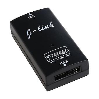
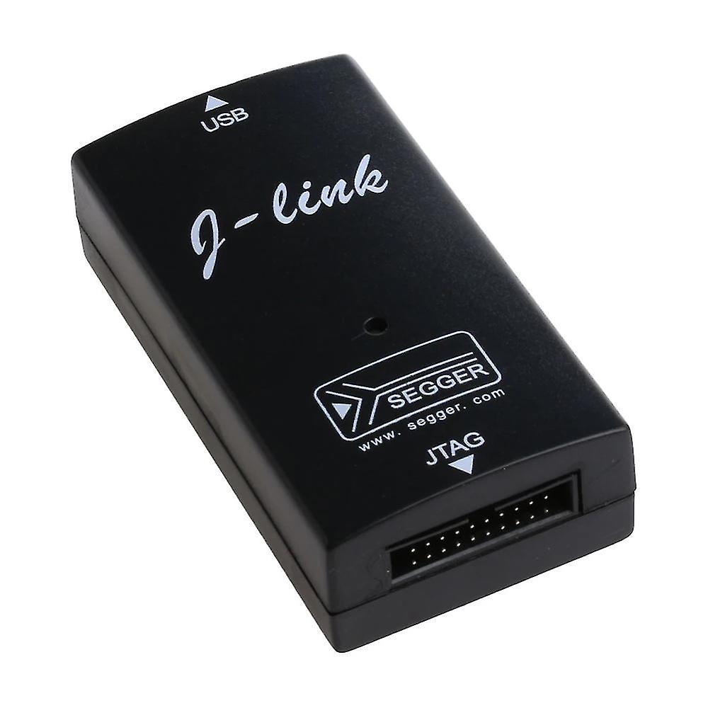
Supported CPUs: AR-M7/9/11, Cortex-A5/A7/A8/A9, Cortex-M0/M1/M3/M4/M7, Cortex-R4, Microchip PIC32 and Renesas RX100/RX200/RX610/RX621/RX62N/RX62T/RX630/RX631/RX63N Differences between JLink V8 and JLink V9: 1. Different speed :V8 supports 10M(JTAG debugging mode)/4M(SDW debugging mode) at most, while Jlink V9 supports 20M (JTAG debugging mode)/ 15M (SDW debugging mode). 2. Different stability: the driver IC of V9 has the voltage adaptive ability, which automatically ADAPTS to the CPU voltage of the target board under the condition of correct wiring. The cpus of 1.8-5.5v can be debugged, while the V8 version can only debug the cpus of 3.3v, and the stability of the debugging 5vcpu is very poor. 3, JlinkV8 easy to drop firmware into a brick. I have a lot of V8 has failed, I need to re-burn the firmware, and ordinary users can only look at the transformation of bricks, and V9 basically no such situation. 4, some of the latest cpuV8 no longer support, and V9 support almost all ARM CPU. JLINK V9 main features: 1. The main control chip adopts STM32F205 without dropping firmware, and the hardware is upgraded to the latest version of V9.4 2. The current of 3.3v voltage 0.8a can be provided for the development board (foot 2) 3. Support standard JTAG interface and 2-wire SWD debugging interface. The speed can reach 20M(JTAG)/15M(SWD) per second. 4, support ARM all chip debugging, support MDK or IAR, and other standards JLink support the compilation environment IDE. 5, original firmware, firmware automatic upgrade 6, gold sinking process, comparable to the original.There are generally three types of power supply: 1. Use the 5v-supply pin to supply power to MCU through the LDO of the target board. 2. Directly connect the VoUT pin to t to the VCC of MCU for power supply. 3. The user can also select the target board with its own power supply. Note: the VTREF pin must be connected to the MCU's VCC regardless of the mode of power supply.
-
Fruugo ID:
208583566-444316050
-
EAN:
9140180230772